This post is the second part of the two-part Harmonics & BLE blog post. We urge you to read this part if you enjoyed Harmonics Part 1 – Introduction to Harmonics & BLE or you didn’t read part 1 but are somewhat familiar with RF emissions and harmonics.
We hope that in part 1 you learned what spurious emissions are, why they can be harmful, and what the FCC does to protect the EM spectrum from excessive spurious emissions. However, what should you do if you’re one of the unlucky people who get to revisit the drawing board after discovering too late in the game that you can’t sell your product because it generates those pesky spurious emissions at too high of a level?
That’s precisely what Punch Through aims to teach you — where some unfortunate emissions may be coming from, some remedies for stopping them, and where to turn for help if needed!
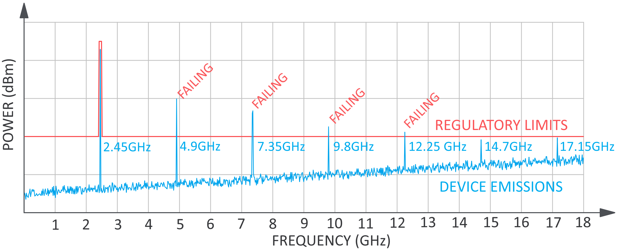
Figure 1 above depicts a scenario that is failing an intentional radiator test. If you find yourself in this unfortunate situation, the first thing you need to do is make an attempt at understanding how the emissions are generated. There are really only two mechanisms on how a device is generating the spurious emissions:
- The device is generating spurious emissions even when it’s not actively transmitting — usually due to noisy power supplies, high-speed signals, or other signal integrity issues.
- The device generates spurious emissions only when the device is actively transmitting — usually due to one of two possible causes:
- The power supply line that powers the radio contains high-frequency noise that causes the radio’s power amplifier to generate harmonics due to inadequate power supply rejection (PSR)./li>
- The fundamental transmit frequency radiates from the device’s antenna and then is picked up by some component or trace (mock-antenna) on the PCB, which then generates the harmonics. This is also a common cause of receiver self-quieting as previously discussed.
Knowing there are only two mechanisms of the device generating spurious emissions, you will want to answer the following questions:
- Was it a failure during the intentional radiator test?
- Was it a harmonic of your radio’s transmission frequency?
If the answer is yes to both of those questions, the harmonics are likely coming straight out of your radio’s RF port, and you have a few things to try:
- If you have a low duty cycled device, Duty Cycle Correction Factor (DCCF) for intentional radiators may be applicable — DCCF is discussed in more detail in a section below./li>
- Reduce maximum transmit power if it is acceptable to the system./li>
- Filter out harmonics from radio’s RF port
If your device failed during unintentional radiator tests or the failing frequency wasn’t a harmonic of your radio’s transmission frequency, fixing the issue may become a little less obvious. The main things to check and test are:
- Identify if any components on your PCA could be generating the failing frequency as a harmonic. If so, verify that the component is the source and fix it, e.g., shielding, filtering, bypassing, termination, layout modifications.
- Use a near-field probe to identify the emissions source and again, fix it (shielding, filtering, etc.) — more on near-field probes in a section below.
As you may already be aware, there is a lot to consider when dealing with spurious emissions, including possibilities as to why they are being generated in the first place. The flowchart depicted in Figure 2 below is intended to help guide you through the process of getting to the bottom of those pesky spurious emissions. Take note that some other possible decisions and methodologies could be used.
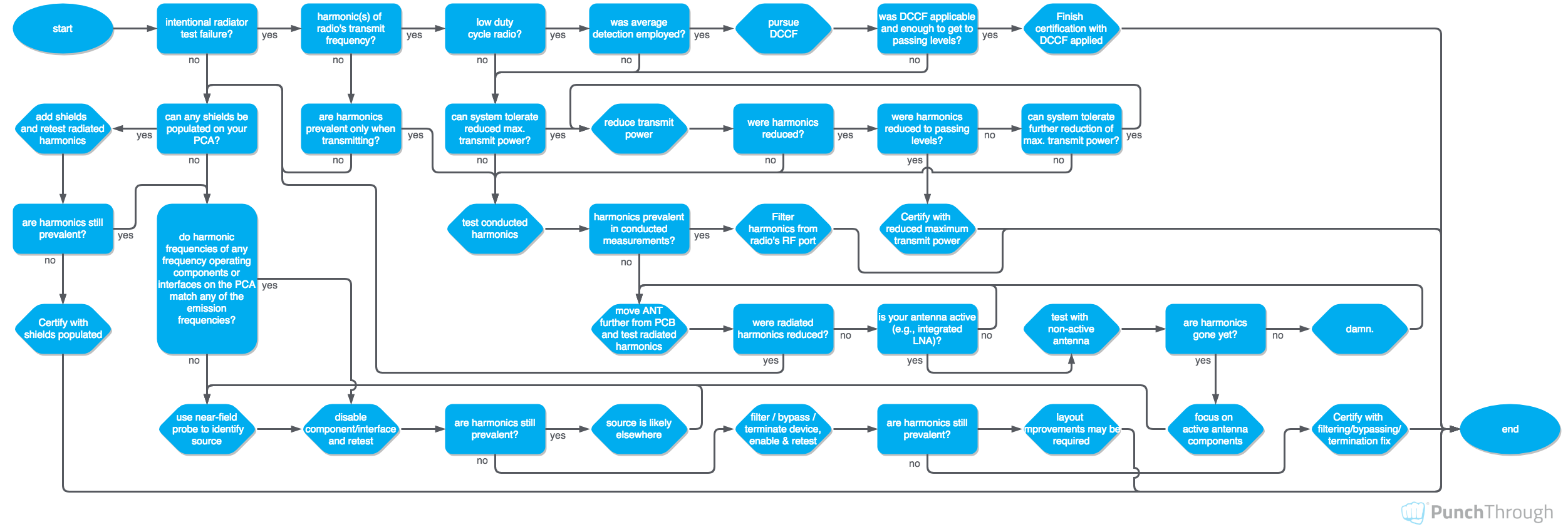
The following sections elaborate on some of the key items mentioned in the flowchart that may help get your device passing FCC tests after it has failed.
Duty Cycle Correction Factor (DCCF)
Under the FCC’s wall of text pertaining to the classification of radio frequency devices (Title 47 Part 15) there exists a small section where BLE radios fit in: §15.249 [Note: BLE devices almost fall under §15.247, but that section requires a device to hop between a minimum of 15 channels, whereas a BLE device will only hop between the 3 advertisement channels while it is advertising or in beacon mode].
The harmonic limit levels specified in §15.249 are expressed as average values as defined by §15.35 paragraph (b). §15.35 paragraph (c) states that when the radiated emission limits are expressed in terms of the average value of the emission, and pulsed operation is employed (such as BLE), then an average value may be calculated from a peak measurement.
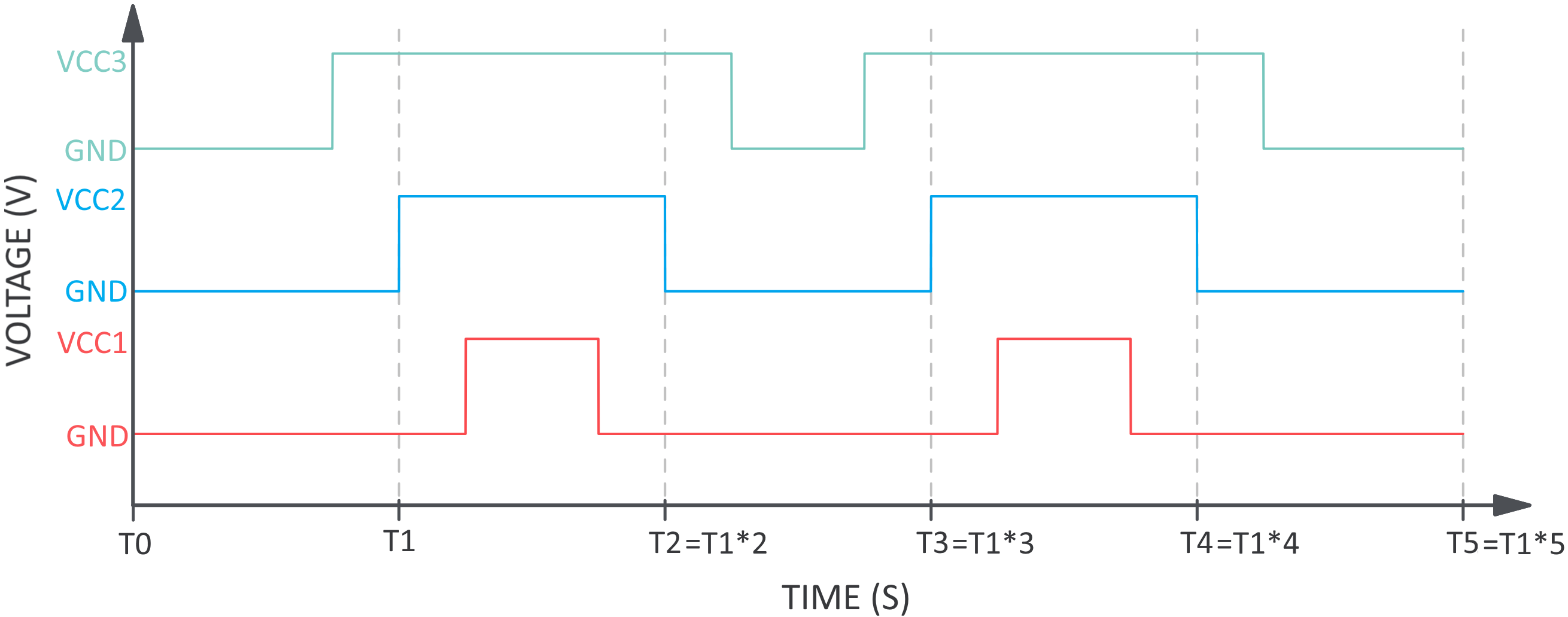
The method commonly used to convert a peak measured value into an average value is calculating and applying a DCCF. The Duty Cycle aspect of DCCF is just a ratio of on-time to off-time. For example, a transmitting signal that is on for 10 milliseconds, off for 90 milliseconds, on for 10 milliseconds, and so on would have a Duty Cycle of 0.1 or 10%. Figure 3 below depicts three different duty-cycled signals of 25% (bottom), 50% (middle), 75% (top):
The Correction Factor aspect of DCCF is just using the duty cycle information to convert a peak measurement value into an average value. Using a known duty cycle ratio and a peak emissions value expressed in volts on a decibel scale (e.g., dBµV or decibel-microvolts), we can use the following equation to determine a DCCF:
- DCCF [dB] = 20 * log (1 / DutyCycle) where 0 < DutyCycle < 1
If we were working with power units on a decibel scale (e.g., dBm or decibel-milliwatts) we would instead use:
- DCCF [dB] = 10* log (1 / DutyCycle) where 0 < DutyCycle < 1
We would then take our peak measured value and reduce it by our calculated DCCF to obtain an average value and make sure the calculated average is below the FCC’s defined average limits.
- Calculated Average Emission [dBµV/dBm] = Measured Peak Emission [dBµV/dBm] – DCCF [dB]
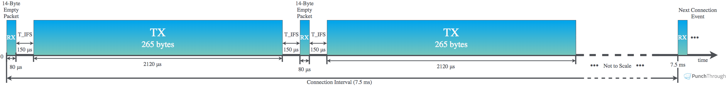
Now we’ll run through the numbers to figure out the DCCF for a BLE radio utilizing data length extension. A different blog post explains the data length extensions feature of BLE v4.2 & v5.0 in much more detail, but it essentially allows the data payload of each packet to increase from the previous 20-byte limitation to up to as much as 244 bytes. Our previous blog posts, Maximizing BLE Throughput on iOS and Android and Maximizing BLE Throughput Part 2: Use Larger ATT MTU, describe the legacy scenarios in great detail as well. To provide a DCCF example in this blog post, consider the following scenario, as illustrated in Figure 4 below:
- Data Length Extension enabled
- Data Rate = 1 Mbit/s OR 1*10^-6 seconds/bit OR 1 µs/bit
- Transmission bits per Packet = 265*8 = 2120 bits/packetTransmit Time per Packet = 1 µs/bit * 2120 bits/packet = 2120 µs/packet
- Packets Per Interval = 2
- Connection Interval = 7.5 ms
- Emission measurements made on a dBuV/m scale (electric field strength)
Using this information, we can determine the transmitting duty cycle as follows:
- DutyCycle = Transmit Time per Packet in seconds * Packets per interval / Connection Interval in seconds
- DutyCycle = 2120µs * 2 / 7.5 ms ≈ 0.57
And now the DCCF can be calculated, using the 20*log(1/DutyCycle) equation because of dBµVm electrical field strength scale:
- DCCF = 20 * log(1/0.57) ≈ 5dB
Using this DCCF value, you can then convert a peak emission measurement into a calculated average value. Let’s say for simplicity’s sake, the average value limit is 10 dBµV/m and the EUT’s measured peak emissions were 11 dBµV/m — failing by 1 dB. The calculated DCCF of 5 dB could then be applied to the measured peak emissions of 11 dBµV/m to convert to calculated average emissions of 6 dBµV/m, now passing by 4 dB. A+!
Of course, there are other possible outcomes of this calculation for other BLE applications, but if you can guarantee that the above calculation represents the maximum transmitter duty cycle for your application then you can reduce peak emission measurements by 5 dB to obtain an average value.
But, what if subtracting the DCCF from the peak measurements wasn’t enough to get your device’s emissions to a passing level? Well, you could further reduce the transmission duty cycle to get a larger DCCF which will hopefully be enough to get your device’s emissions to a passing level — assuming your application can tolerate the reduction, which likely means reducing data transfer rates. But at this point, it might be worth taking a step back to try to reduce the peak emissions by other means, such as reducing your device’s maximum transmit power or trying to understand where the emissions are being generated so they can be mitigated at the source.
Digesting the frequency content of spurious emissions plots
When looking at spurious emission plots such as the examples shown in part 1 of this blog post it can sometimes be overbearing, but most of the time you will start to notice some of the “spikes” in the plot appear to be evenly spaced and seem to be harmonics of their frequency delta. While this is a great thing to notice, it can sometimes be misleading.
Ideal digital signals (a.k.a. square waves, or more appropriately trapezoidal waves) when represented in a frequency domain are naturally composed of odd harmonics of their operational frequency (lookup Fourier Series and check out this Fourier applet if you aren’t familiar with this concept). A very common digital signal for communication interfaces in electronics is the Serial Peripheral Interface (SPI). One of the signals in the SPI protocol is a clock signal which is shown as an example below and always toggles between logic low and logic high with some amount of transitional time between the two logic levels. The trapezoidal wave shown in Figure 5 below is the SPI clock in the time domain — let’s assume with a frequency of 1 MHz and a rise time of 10 ns. Figure 6 below shows this same trapezoidal SPI clock, but in the frequency domain — let’s assume the pulses are spaced by 2 MHz and are the odd harmonics (3rd, 5th, 7th, etc.) of the 1 MHz SPI clock. Note that extrapolation was applied between some harmonics for simplification. Knowing that only odd-order harmonics may appear in emissions plots can help when trying to quickly identify the noise source — such as a 1 MHz SPI clock in this case when only spikes spaced by 2 MHz appear in the plot.

Another thing to be aware of when quickly looking at spurious emission plots is the scale used for the frequency axis — the unevenly spaced harmonics plotted above in Figure 6 are on a logarithmic frequency scale which is common when dealing with unintentional and intentional radiator test plots. The visual spacing of harmonics that appear on a logarithmic scale will decrease as frequency increases.
Conducted Measurements
Conducted measurements can be very helpful in producing repeatable bench tests if you don’t have access to an RF anechoic chamber even at a small scale. A conducted measurement takes your device’s antenna out of the equation so you can determine what exactly is being generated from the RF port of your radio circuit before it turns into energy radiated from your device’s antenna. This is done by disconnecting your device’s antenna from the radio’s RF port and connecting it directly to a Spectrum Analyzer, Signal Generator, Power Meter, or a high-end Communications Tester via a coaxial cable. This can be done by physically replacing the antenna with the coaxial cable and test equipment or by using an RF switch if one was designed into the circuitry specifically for this purpose as the sketch shows in Figure 7 below.
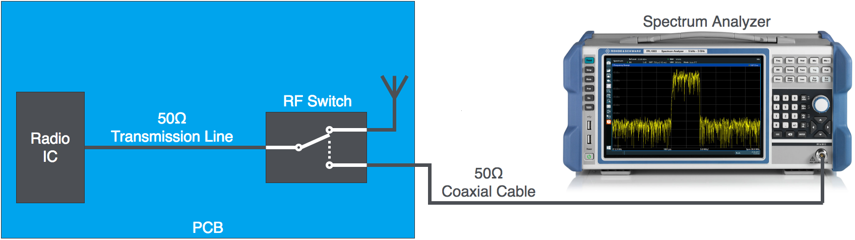
This type of measurement setup helps debug spurious emissions that are emanating from your radio’s RF port. Conducted measurements are also essential in verifying other RF performance parameters of your device’s radio such as transmit power level, receiver sensitivity, and error vector magnitude (EVM).
Power Supply Noise
Feeding the power amplifier in a radio with a noisy supply voltage is a common cause of pesky harmonic emissions appearing at the RF output port of your radio. Figure 8 below shows the mechanism of how relatively low-frequency noise on a power supply (ƒSW) shows up as harmonics near the much higher carrier frequency output (ƒ0).
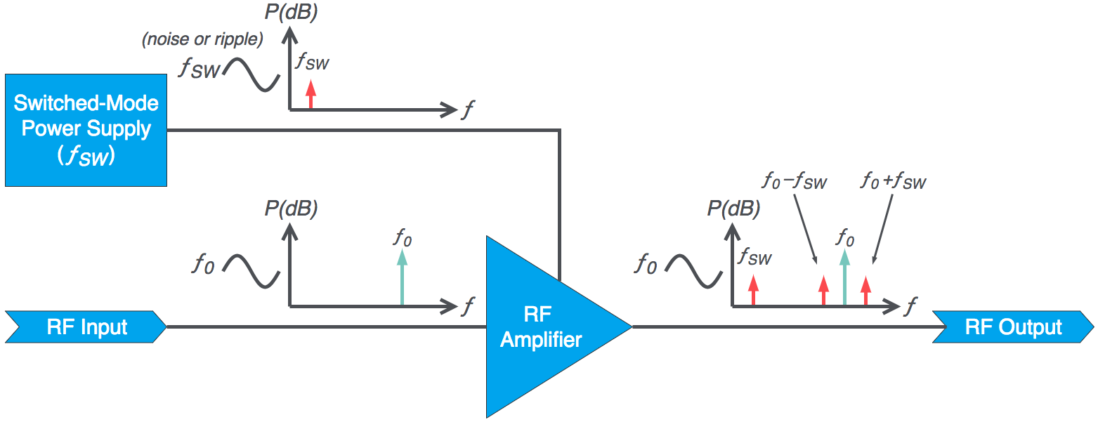
If these harmonics are far enough away from your radio’s RF board (f0-fSW << f0 << f0+fSW) then they can sometimes simply be filtered at the RF output. However, with this type of harmonic generation, the frequencies of these harmonics are typically too close to the RF output and filtering the harmonics would also filter the carrier frequency at the RF output. In this case, the noise must be removed from the voltage supply — power filtering is usually the easiest option but sometimes you may need to add an RC snubber circuit, choose a linear voltage regulator, which is not noisy, and have good PSRR (power supply rejection ratio), or even improve the PCB layout around the power supply and RF circuit.
Near-field Probe

A near-field probe is essentially a bad antenna — it only couples with an EM field when it is within several inches of the strong EM radiation source. By connecting a near-field probe to a spectrum analyzer, one can see EM radiation frequencies emanating from a source close to the near-field probe. This is sometimes extremely helpful when an emission source needs to be identified to a specific location on a circuit and other methods have been unsuccessful. Near-field probes come in various shapes and sizes shown in Figure 9 below.
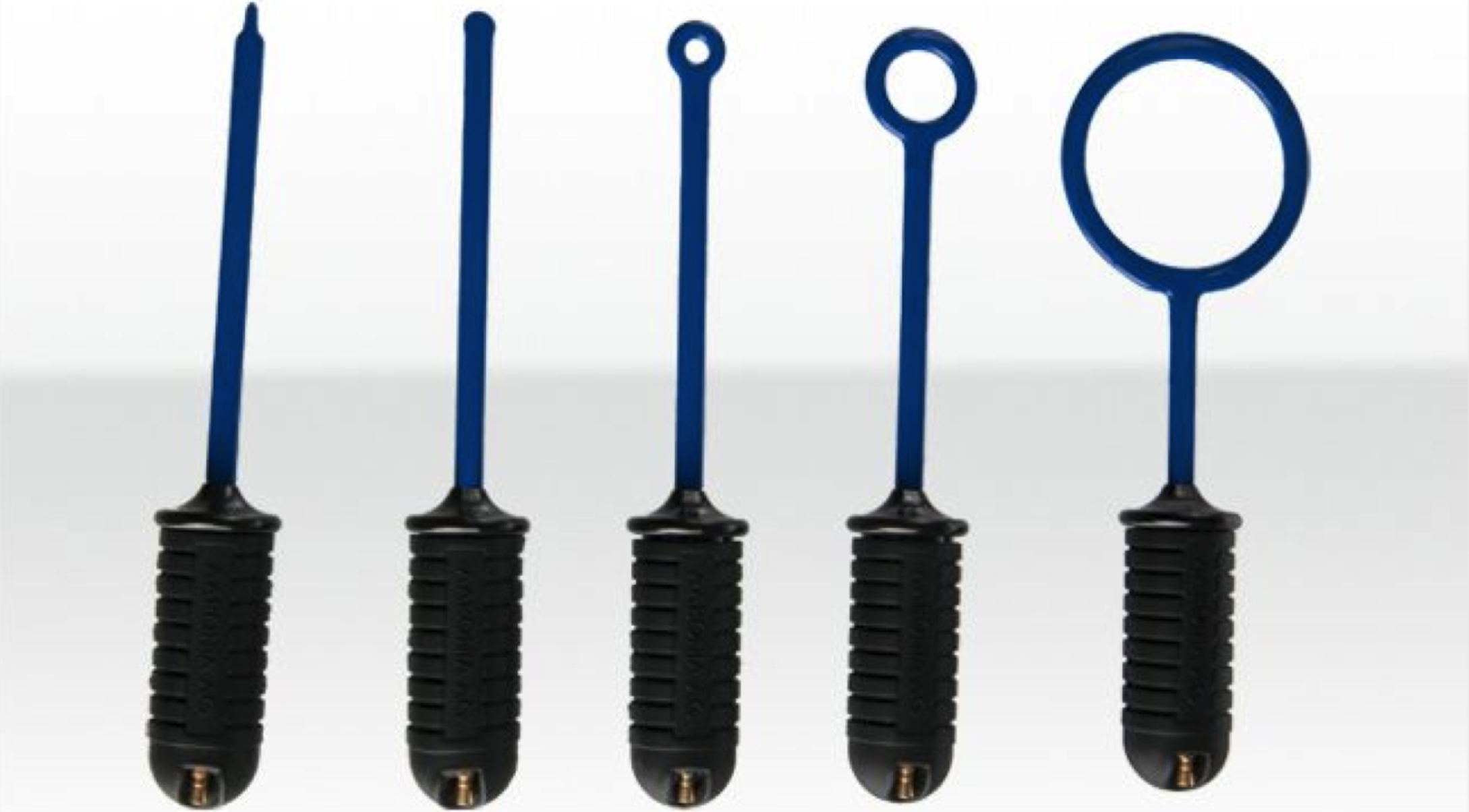
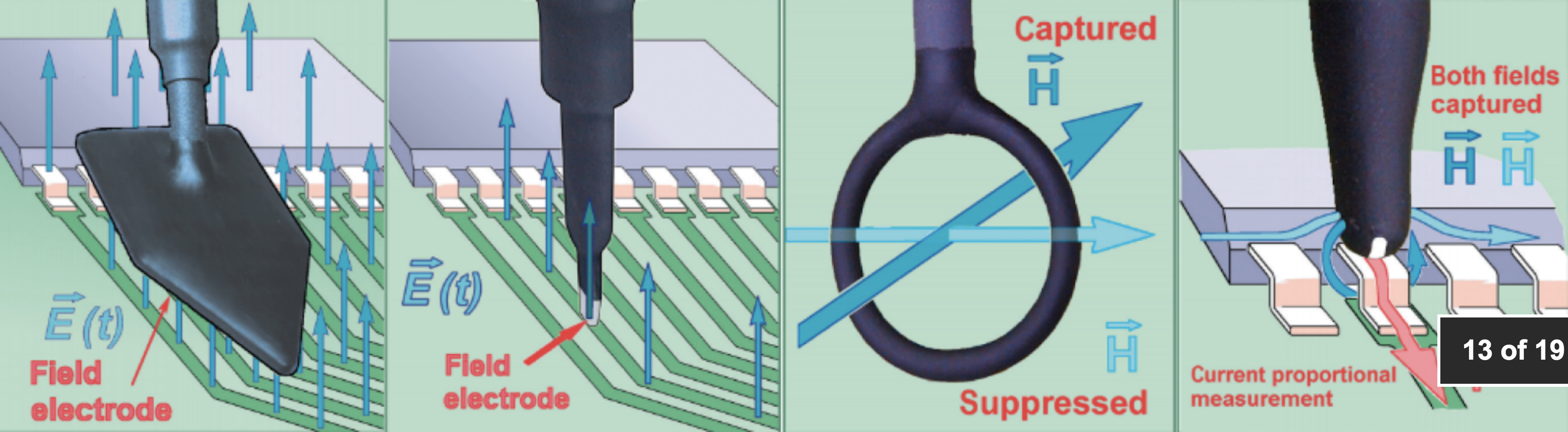
The different shaped near-field probes all have different purposes. Figure 10 below shows what EM fields will be picked up by different probe types. Remember that an EM field is composed of an Electric Field (E-field) and a Magnetic field (H-field)? Well, the fine tip probes only couple with E-fields in a very small area at close distances — useful for detecting E-fields from a small area such as a single PCB trace. The metal detector shaped probes detect E-fields more easily — useful for quickly “sweeping” for E-fields over a larger area such as an entire PCB. The donut-shaped probes only couple with H-fields — smaller donuts have smaller detection area and are useful for narrowing in on the H-field source.
When dealing with very low power emissions, such as ones that typically cause self-quieting, a spectrum analyzer may not be able to detect the weak signal picked up by the near-field probe. In these cases, a wideband low-noise amplifier (LNA) may be required to amplify the weak signal picked up by the near-field probe so a spectrum analyzer detects the signal.
Having Self-Quieting Problems?
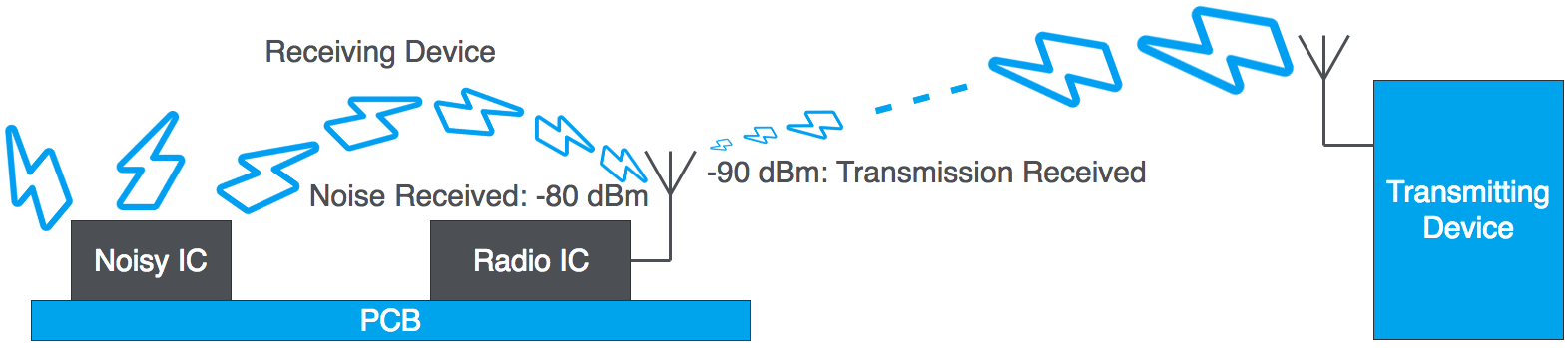
Self-quieting is a problem you face when your wireless electronic is generating spurious emissions at frequencies in your radio’s frequency band — 2.402 GHz to 2.480 GHz in the case of BLE — and are high enough intensity to be picked up by your radio’s antenna. This causes receiver sensitivity performance issues that are usually ineptly blamed as “poor range” or “bad antenna”. This self-quieting scenario is illustrated in Figure 11 below where the “lightning bolts” represent EM field intensities. Self-quieting is no easy issue to overcome — fixing and/or avoiding these issues is the full-time job of some RF engineers.
Usually, the first thing you want to do is verify that self-quieting is actually the reason for your radio’s reduced sensitivity or range. You can get as sophisticated as you want with tests to diagnose self-quieting, but at the most basic level you will need a controlled environment where your tests are repeatable. Highly sophisticated test setups also usually imply highly expensive test setups, so the list below will include examples of both basic and sophisticated options of a test setup for diagnosing self-quieting:
- RF isolation: large open field (basic) or RF anechoic chamber (sophisticated)
- Signal generator: known good test unit with no RF performance issues (basic) or a wireless communications tester (sophisticated)
- Ability to control power level incident to the receiver of the Electronic Under Test (EUT): adjust distance between transmitter and receiver (basic) or adjust transmit power level of signal generator (sophisticated)
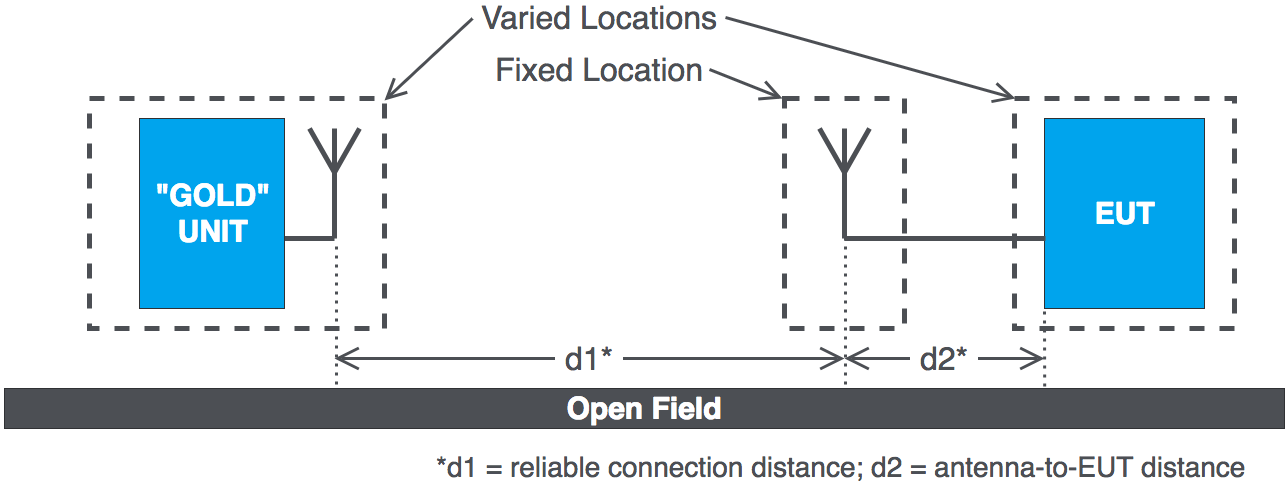
In a basic test setup example as depicted in Figure 12 below, follow these steps to diagnose self-quieting:
- Find a large open and flat field – minimum size of a soccer field but longer and wider than the expected range of the EUT
- Place the EUT at a fixed location on one end of the field.
- Move the golden unit towards the other end of the field (away from the EUT) until they barely maintain a connection. The distance between the EUT and golden unit at this location is distance d1.
- Increase distance d2 between the EUT and the EUT’s antenna while keeping the EUT’s antenna in a fixed position — the larger the distance the better but aim for at least a few feet.
- Check to see if the reliable connection distance d1 can now be increased by moving the golden unit further away from the EUT’s antenna.
- Did distance d1 increase a noticeable amount? If so, the EUT was having self-quieting issues that were alleviated by moving the EUT’s antenna further from the EUT’s noise source.

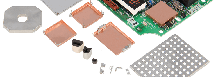
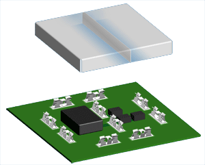
If your system can simply accept moving the antenna further from the circuit board, then the case is closed. But this is unacceptable in most cases, especially when the antenna is integrated on your circuit board as opposed to an external cabled antenna. When you can’t just move the antenna further from the circuit board, the self-quieting emissions must be stopped from reaching the radio’s antenna by other means. One common option for this is adding shields around likely noise sources on your PCB: processors, high-speed memory, clocks, switching power supplies, cables, other digital signals with fast rise-times. Having the foresight to create placeholders for adding shields when designing the PCB can be a lifesaver under these circumstances — examples of shielding placeholders and materials are shown in Figure 13 and Figure 14 below.
[image courtesy of Holland Shields]

[Animated GIF courtesy of Holland Shields]
When adding a shield isn’t feasible or adding it didn’t turn out to be helpful, the next step is to hone in on the source of the self-quieting emission. If you’re lucky, you may be able to find the source of the self-quieting emission using a near-field probe and spectrum analyzer (as further described in the Near-field Probe section below). If you’re unlucky and the emission level is too low to measure with a near-field probe, or the components are too small and tightly spaced where a specific component can’t be identified as the source with a near-field probe, then what?
Well, then you’ll have to start getting even more creative, be well versed with a soldering iron, and not be afraid to hack at traces or components on your circuit board. What components of the circuit can be shut off or removed while still keeping the radio functional? If you shut down the analog section on your circuit board and all of sudden the receiver’s sensitivity improves, then you know the analog section is generating the self-quieting spurious emission. If you then take a step back and only disable the SPI signals to the analog section and the sensitivity is still improved, you know the SPI signals are to blame for your troubles.
So, you found the culprit, now what?
There are many root causes of unintentional spurious emissions and many ways to suppress those spurious emissions at the source. Below are some examples of root causes and their potential suppression methods.
Digital signals with fast logic level transition times:
- Slow down the transition times with high-frequency filtering.
- Prevent harmful signal reflections by providing proper resistive termination.
Noisy power supply outputs or RF noise coupling into IC power inputs
- Filter power supply outputs with feed-through capacitors or ferrite beads.
- Provide localized bypass capacitance for all IC power inputs.
Poor PCB layout / stack-up techniques for high-speed signals or power supplies:
- Minimize return current paths for all signals with fast logic level transitions.
- Avoid breaks or slots in power and ground planes — these are just asking for EMI. Where breaks or slots in power planes are required, route high-speed signals around the break.
- Have a minimum of one layer as a dedicated ground plane. As the signal layer count goes up, more dedicated ground plane layers are advised.
Lack of cable filtering, especially for cables with high-speed or high-power signals:
- Add ferrite clamps on the cable.
- Add ferrite beads, feed-through capacitors, or RF bypass capacitors on the PCB near the cable’s connector.
- Control the return current path — sometimes distributing multiple power or ground connection points can cause more harm than good.
Parting words…
As mentioned previously in this blog post, some RF Engineers spend their whole career focused on preventing and suppressing spurious emissions — it can be a daunting task resulting in many PCB revisions with little to no improvements for the inexperienced. Punch Through is always here to help and ready to step in at any stage of the game — be it design reviews early in product development or suppressing that stubborn harmonic discovered during FCC testing. We have a team of engineers well-versed in design best practices and suppression methods for an EMI-friendly product!